Tesla’s Dojo is the world’s most advanced and scalable AI training machine. Tesla debuted its Dojo supercomputer technology at its AI Day, showcasing its growing in-house chip design talent. The manufacturer claims to have created the world’s fastest AI training machine. Tesla has been touting the creation of an in-house supercomputer designed for neural net video training for years. Tesla’s neural networks are trained using a massive quantity of video data from its fleet of over 1 million vehicles.
The automaker was unhappy with the current hardware solutions for training its computer vision neural nets and believed it could do better internally. Elon Musk, Tesla’s CEO, has teased the creation of Tesla’s own supercomputer, dubbed “Dojo,” for the past two years. He even indicated last year that Tesla’s Dojo will have a capacity of more than an exaflop, or one quintillion (1018) floating-point operations per second, or 1,000 petaFLOPS. It has the potential to make Dojo the world’s most powerful supercomputer.
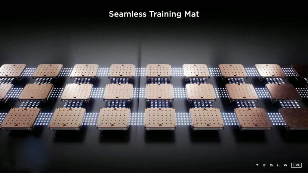
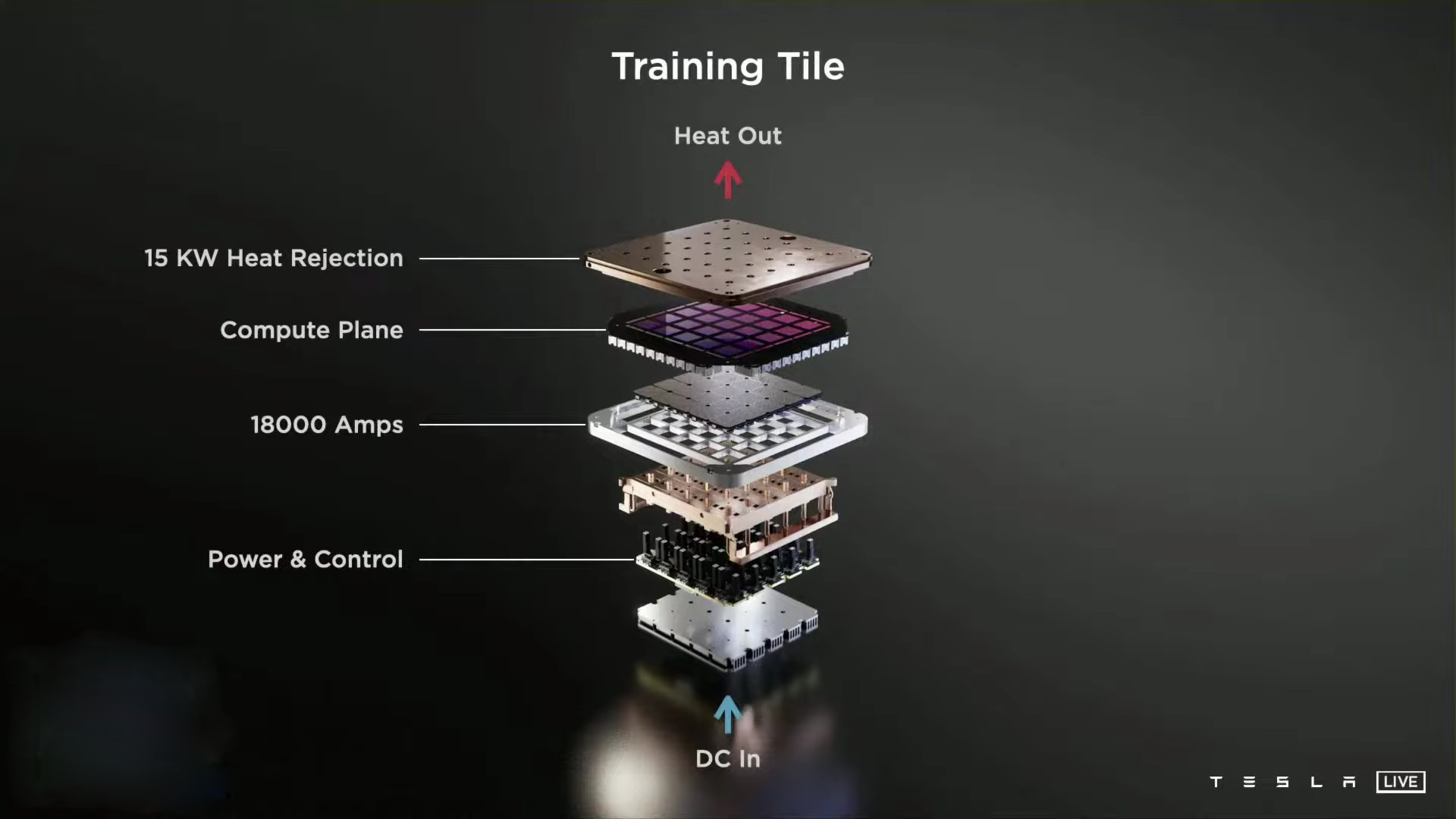
The presentation was led by Ganesh Venkataramanan, Tesla’s senior director of Autopilot hardware and the project’s head. The engineer began by demonstrating Dojo’s D1 chip, which uses 7-nanometer technology to give unprecedented bandwidth and computation capability. The chip was meant to “seamlessly link without any glue to each other,” and Tesla took advantage of this by connecting 500,000 nodes. It combines the UI, power, and thermal management to create what it refers to as a training tile.

Also Read:
Fugaku – Fastest Supercomputer in the world today
[email-subscribers-form id=”1″]
In a less than 1 cubic foot configuration, the outcome is a 9 PFlops training tile with 36TB per second of bandwidth. However, in order to properly build the first Dojo supercomputer, it still needs to form a compute cluster utilizing those training tiles. Tesla hasn’t finished building the system yet, but CEO Elon Musk has stated that it will be operational next year.
In May 2020, Nvidia launched the A100 AI chip, which has 54 billion transistors and a performance of 5 petaflops.
Tesla’s current HPC capabilities are impressive. In June, Tesla’s senior director of AI, Andrej Karpathy, disclosed the details of the company’s unnamed pre-Dojo supercomputer.
This cluster, one of three run by the corporation, contains 720 nodes, each with eight 80GB Nvidia A100 GPUs, for a total of 5,760 A100s in the system. Based on past A100 performance benchmarking on Nvidia’s own 63 petaflops Selene supercomputer, 720 sets of eight A100 nodes may deliver roughly 81.6 Linpack petaflops, putting the machine fifth on the most current Top500 ranking.

The D1 chip is manufactured in seven-nanometer technology it packs 50 billion transistors in a miserly 645-millimeter square. A hundred percent of the area is going towards machine learning training and bandwidth and there is no dark silicon there is no legacy support this is a pure machine learning machine. The chip was entirely designed by tesla team internally all the way from the architecture to package.
The chip is like a GPU level compute with a CPU level flexibility and twice the network chip-level i/o bandwidth. Since d1 chips can seamlessly connect without any glue to each other we just started putting them together we just put 500 000 training nodes together to form our compute plane, explained Ganesh Venkataramanan during the presentation. In order to achieve this compute plane
Tesla had come up with a new way of integrating these chips together, to build a Tile. This is a pioneering integration of 25 known good d1 dies onto a fan-out wafer method tightly integrated such that the bandwidth between them is preserved, and in addition, the maximum bandwidth is preserved there. This approach gives us nine petaflops of computing and a high bandwidth high-density connector that retains the bandwidth flowing out of this training tile, he added.

It was not easy to design this because there were no tools available, and all of the tools were failing. Even our compute cluster couldn’t handle it, so our engineers had to come up with new approaches to make this a reality, he said. Tesla also came with a new way to feed power to this in a vertical way. They created a custom voltage regulator module that could be reflowed directly onto this fan-out wafer. Also, integrated
the entire electrical thermal, and mechanical pieces to create a completely integrated interface system with a 52-volt dc input for training tile. “It’s unprecedented this is an amazing piece of engineering our compute plane is completely orthogonal to the power supply and cooling that makes high bandwidth compute planes possible,” he said.
Scalability
The 9 petaflop training tile becomes the unit of scale for this system. Tesla engineers then put together some tiles, a two by three tile in a tray to make the training matrix, and two trays in a cabinet
gave 100 petaflops of compute. They did not stop here, then they broke the cabinet walls we integrated these styles seamlessly all the way through preserving the bandwidth, all the tiles are
seamlessly connected with the same bandwidth and created an exopod. The exopod gives one exaflop of compute in 10 cabinets.
The compute plane can be subdivided can be partitioned into units called dojo processing unit a DPU consists of one or more D1 chips, it also has an interface processor and one or more hosts. This can be scaled up or down as per the needs of any algorithm any network running on it.

Watch the complete presentation below:

