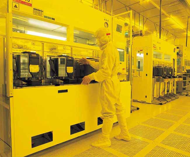
TSMC Has Started Development Of A 1.4-nm Chip Fabrication Process.
In June, TSMC is expected to convert its 3-nm process R&D team to a 1.4-nm process R&D team.
According to Business Korea, the company has started developing a 1.4-nm chip fabrication process.
By announcing the start of a quest to build a 1.4-nm chip fabrication technology, TSMC has triggered technological competition once again. As a result, Samsung Electronics, which trails TSMC in the worldwide foundry industry, has no alternative but to react to the market leader’s approach.
Samsung, on the other hand, has been pursuing TSMC with vigor. In 2022, the business plans to mass-produce 3-nm goods employing a next-generation transistor structure called gate-all-around (GAA). This method reduces the size and speed of transistors. Samsung is on the verge of commercializing the technology before TSMC.
Intel is a newcomer to the technology competition. It revealed plans to build a sub-2-nm technique before TSMC and Samsung. Intel stated its intention to return to the foundry business in 2021. In the second half of 2024, it also promised to mass-produce 1.8-nm items.
Industry observers, on the other hand, are doubtful. Foundries are currently having difficulty with ultra-micro manufacturing methods. As a chip’s size decreases, the circuit must be drawn more precisely. The technological obstacles are continually rising. Yield management is becoming increasingly complex, Business Korea reported.

