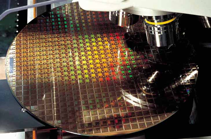
TSMC’s 3 nm process facility structure completion, to start production by second half of 2022
Taiwan Semiconductor Manufacturing Company, Limited (TSMC) achieved a significant milestone in completion of their 3 nm fab facility at the Tainan’s Southern Taiwan Science Park on Nov 24, 2020.
Mark Liu said, the factory will be the worlds most advanced logic process plant and help company maintain its leading position in the semiconductor industry, CNA reported.
In semiconductor manufacturing, the 3 nm process (3.5nm) is the next die shrink after the 5-nanometre MOSFET (metal–oxide–semiconductor field-effect transistor) technology node.
[monsterinsights_popular_posts_inline]
As of 2019, Samsung and TSMC have announced plans to put a 3 nm semiconductor node into commercial production. Samsung’s 3 nm process is based on GAAFET (gate-all-around field-effect transistor) technology, a type of multi-gate MOSFET technology, while TSMC’s 3nm process will still use FinFET (fin field-effect transistor) technology, despite TSMC developing GAAFET transistors.
************************************************************
Subscribe to our newsletter for latest updates:
************************************************************
Specifically, Samsung plans to use its own variant of GAAFET called MBCFET.
Earlier this year Samsung had announced to deliver the 3 nm manufacturing in 2022. Samsung is working on Gate-All-Around FET technology. Once mass production begins, TSMC expects capacity will exceed 600,000 12-inch wafers per month, Liu added.
TSMC’s process will create in upwards of 250 million transistors per mm2. With 3 nm process, 300 million transistors per mm2 is achievable, that would give around 90 billion transistor density.
TSMC produces chips for Apple, AMD and NVIDIA. AMD Ryzen CPU’s and Radeon GPU’s are produced by TSMC. Also, Apple chips are produced by TSMC.
Performance:
TSMC says the 3nm has a 1.7x density improvement over the 5nm process performance is 5% higher than 5nm and energy consumption increased by 15%.
As per TSMC, will conduct, 3 nm (N3 node) risk trial production in 2021 and mass production will commence in the second half of 2022.
Also Read: Cerebras wafer size chips faster than real time? Cerebras CS1 fastest & largest chip
